CINNO Research, Dainippon Printing Co., Ltd. recently announced that it has developed a new generation of interposer for semiconductor packaging.
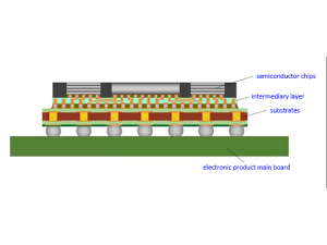
According to the official website of Dainippon Printing, the semiconductor market is expected to grow further with the development of digital transformation (DX) worldwide, especially with regard to the next generation of communication systems and artificial intelligence (AI) for 5G and post-5G, which will place higher demands on semiconductor products. To achieve high functionality, high speed and low power consumption performance of semiconductor products, miniaturization process development of silicon wafers is required, but complex processes and high costs are pushing the development of miniaturization close to its limits. In this case, a new generation of packaging technology is attracting attention as a way to further improve performance. The approach is to mount multiple chips with different functions, such as CPUs and memories, on the same substrate in high density to increase processing speed. DNP has developed a relay element “intermediate layer” that plays a key role in packaging technology and electrically connects multiple semiconductor chips to the substrate.
DNP has also developed “microfabrication technology,” which is the core of the printing process, and applied it to the manufacture of “photomask” boards for patterning semiconductor circuits, “stencils” for nanoimprint lithography for next-generation pattern transfer, and foundry services for sensor MEMS. We have succeeded in developing a high-performance interposer layer by utilizing our glass and silicon substrate processing and handling technologies and microscopic wiring technologies accumulated in our past business.
This intermediary layer solves the problem of “increased wiring resistance and reduced inter-wiring insulation caused by degradation of the wiring layer” that becomes apparent with miniaturized wiring, and realizes the high-performance miniaturized wiring required for next-generation semiconductor packages.
DNP participates in “JOINT2 (Jisso OpenInnovation Network of Tops 2, of which Showa Denko is the president),” a consortium of 12 companies engaged in research and development of semiconductor packaging materials and devices, with the aim of establishing packaging and evaluation technologies for next-generation semiconductors. In preparation for mass production of intermediate layers in 2024. Through the development of JOINT2 and cooperation with participating companies, DNP will continue to promote the functional development and mass production of intermediate layers and contribute to the development of next-generation semiconductor packaging technology.