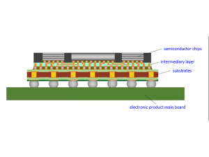
Photoresist is currently widely used in the processing and production of micro-pattern lines in the optoelectronic information industry. The cost of the photolithography process accounts for about 35% of the entire chip manufacturing process, and the time-consuming process accounts for 40% to 60% of the entire chip process. It is in semiconductor manufacturing. Core craftsmanship. Photoresist materials account for about 4% of the total cost of chip manufacturing materials and are the core material for semiconductor integrated circuit manufacturing.
Photoresist is a pattern transfer medium, which uses different solubility after light reaction to transfer the mask pattern to the substrate. It is mainly composed of sensitizer (photoinitiator), polymerizer (photosensitive resin), solvent and auxiliary agent.
The photolithographic collagen materials are mainly resins, solvents and other additives. Among them, the solvent quality accounts for the largest proportion, generally above 80%. Although the proportion of other additives is less than 5%, they are the key materials that determine the unique properties of photoresist, including photosensitizers, surfactants and other materials.
In the photolithography process, photoresist is uniformly coated on different substrates such as silicon wafers, glass, and metals. After exposure, development, and etching, the pattern on the mask is transferred to the film to form and mask. The membrane plate corresponds exactly to the geometrical figure.
Photoresist can be divided into three categories: semiconductor photoresist, panel photoresist and PCB photoresist according to its downstream application fields.
-
Semiconductor photoresist
At present, KrF/ArF is still the mainstream processing material. With the development of integrated circuits, lithography technology has gone from G-line (436nm) lithography, H-line (405nm) lithography, I-line (365nm) lithography, to deep ultraviolet DUV lithography (KrF248nm and ArF193nm), 193nm immersion Type plus multiple imaging technology (32nm-7nm), in the development of extreme ultraviolet (EUV, <13.5nm) lithography, even non-optical lithography (electron beam exposure, ion beam exposure) is used, and the corresponding wavelength is the photosensitive wavelength. Various types of photoresist are also used.
-
Panel photoresist
Photoresist is a key material for LCD panel manufacturing. According to different objects, it can be divided into RGB glue, BM glue, OC glue, PS glue, TFT glue and so on.
Panel photoresists mainly include photoresist for TFT wiring, LCD/TP spacer material photoresist, color photoresist and black photoresist. Among them, the photoresist for TFT wiring is used for ITO wiring, and the LCD/TP precipitation material photoresist is used to keep the thickness of the liquid crystal material between the two glass substrates of the LCD constant. Color photoresist and black photoresist can give the color filter color development function.
-
Photoresist for PCB
PCB photoresist can be divided into UV curing ink and UV spray ink according to the coating method.